S11 of -131522dB and exhibits unconditional stability. My university seems to only have the NCSU CDK tools and libraries.
2
Welcome to the RF Design Tutorials video tutorial series.

. Welcome to our site. To participate you need to register. The proposed LNA is designed using two different tools namely Advanced Design System ADS and Cadence Virtuoso.
Common Source CS LNA. Cadence virtuoso platform. RF Setup f or LNA Analysis i n Cadenc e B.
HiI try to design Ka band LNA in ADS and using cadence to drew layout. Lna is used for impedance matching amp. I am a graduate student who is looking to perform some s parameter analysis on a LNA.
Design an lna using the 90nm. The designed LNA exhibits a gain of 1891 dB. Previous article in issue.
The stability factor K is greater than 1 for the entire range. The technology used for designing is 180nm CMOS. To character the LNA.
The main challenge of LNA design lies in the design of the inputoutput matching network to render Γin and Γout close to zero so that the LNA is matched to the source and load ports. This configuration exhibits high gain and good. According to the configuration the CMOS LNA design can be classified as follows.
Determine the J OPT of the amplifier. Simulator from Cadence Design System. I have shown some hand calculations that I have used and applied these simple concepts to designing a 24 GHz LNA here.
Click here to register now. The 3-dB bandwidth for this LNA design is 57-64 GHz. 18µm RF CMOS features high stability and low power consumption and provides complete design tools services and support including command files for EDA comprehensive technical documents on the manufacturing process.
The standard CMOS technology has revolutionized the transceiver circuits in communication systems. Lna design by tkb sir design prespective iit kharagpur. Have you have any idea about connecting these two software.
Create and draw the schematic LNAas shown in Fig. The layout was also designed with zero errors in both DRC Design Rule check and LVS layout vs schematic check implying that the proposed LNA can be fabricated without any off-chip components. CS LNA with inductive source degeneration.
Designed Cascode LNA is implemented in cadence virtuoso platform using 65nm technology with gain of 15dB. Maintain this current density throughout the rest of the design steps. This is equivalent to solving.
This tutorial describes how to use SpectreRF in Analog Design Environment to simulate parameters which are important in design and verification of Low Noise Amplifiers LNAs. The various performance parameters of the LNA simulated using ADS and Cadence is compared. Floyd 1 3 201 2 1 Please read thr ough the tools se tup document firs t and complet e those steps the fi.
Cadence Design Systems Inc. Lna design tutorial cadence The Cadence IC has a lot RFIC design examples. The components values are listed below.
The baluns used in the testbench are three-port devices. Most tutorials have the schematic drawn with parts from the library called analogLib. With the incorporation of well-designed and optimized narrow-band LNA the receiver.
The technology used for designing is 180nm CMOS. And a whole lot more. Any one help me that i am doing Complemetary current reuse LNA in MICS band in Cadence spectrai selected one IEEE paper regarding my projectIn that they didnot mention any device specification ie value of inductorcapacitorresistorwidth of transistor also i dont know how to desidn these device values alsoMy operating freq is 401-406MHz.
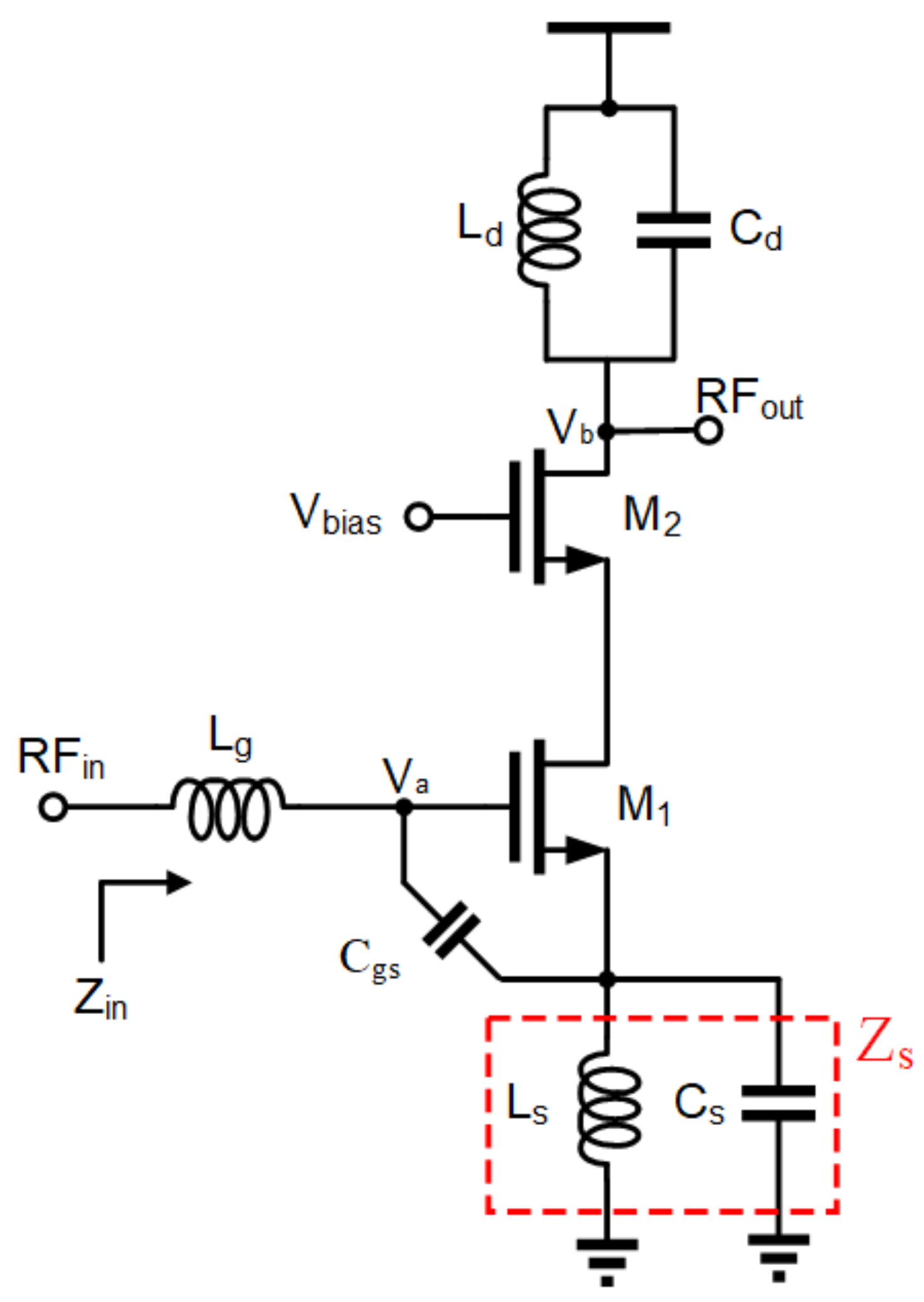
With the knowledge of a generic LNA model Figure 1-3 shows the testbench for a differential LNA. ECE 712 Pro ject 1. M1 M2 200 um035 um choose number of gates to have larger width of transistors Mbias 60 um035 um.
Dec 9 2004 4 V vonleo Member level 1 Joined Oct 30 2004 Messages 34 Helped 1 Reputation 2 Reaction score 0 Trophy points 1286 Activity points 288 cadence lna design. Lna design in cadence Written By puhuyaoma Saturday April 23 2022 Add Comment Edit. Look at the Cadence document and the example.
The version of cadence licensed to my university UMKC is 615. The noise figure is 498 dB at 60 GHz. Make a new library rf_lab1in Cadence Library Manager and attach this library to the TECH_C35B4 technology file.
Cadence customers are the worlds. A LNA has been designed in Cadence simulator in 60 GHz band 57-64 GHz in 65nm CMOS with microstrip as on-chip inductors. Set the V DS of transistor for maximum linearity such that clipping of output is avoided.
FminJ J 0. Design Methodology for CS and Cascode LNA I Step 1. Three power gain definitions appear in the literature and are commonly used in LNA design.
LNA has gain of 1155 dB at 60 GHz. You will be familiar with the Cadence RFIC design tool. Designed Cascode LNA is implemented in cadence virtuoso platform using 65nm technology with gain of 15dB.
About Press Copyright Contact us Creators Advertise Developers Terms Privacy Policy Safety How YouTube works Test new features Press Copyright Contact us Creators. Design Methodology for CS and Cascode LNA I Step 1. In case of CS stage use V DS V DD I Step 2.
Design of a 10GHz LNA for Amateur Radio Operation Using AWR Software Cadence is a pivotal leader in electronic design and computational expertise using its Intelligent System Design strategy to turn design concepts into reality. Narrow-band LNA is the building block of any such CMOS-based receiver. In the 9th video of the series you will learn about practical RF Low Noise Amplifier design flow.
A Schematic Of A Cascode Lna Topology Adopted To Apply The Cnm Download Scientific Diagram
Adaptive Enhancement Of Low Noise Amplifier Using Cadence Virtuoso Tool Semantic Scholar
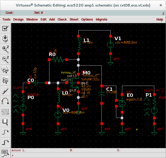
Linear Simulation For An Amplifier Multifunctional Integrated Circuits And Systems Group Mics Virginia Tech

Amplifier Lna Design Question Series Drain Inductor Electrical Engineering Stack Exchange
12 16ghz Lna
Noise Figure Of Differential Signal Rf Design Cadence Technology Forums Cadence Community
Electronics Free Full Text Analysis And Design Of Harmonic Rejection Low Noise Amplifier With An Embedded Notch Filter Html

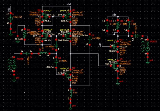
Cadence Circuit Schematic For The Medradio Lna With Integrated Output Download Scientific Diagram
0 comments
Post a Comment